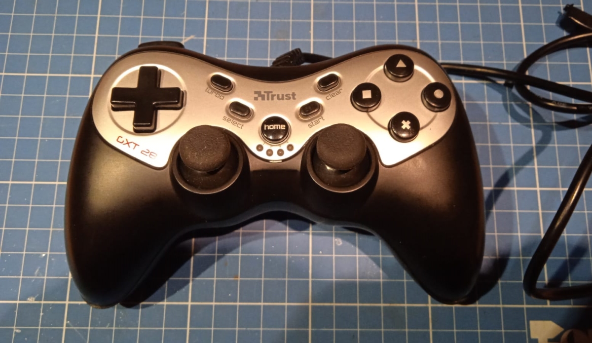
Found this USB game controller at the thriftstore with some fun functions like actual analog feeling triggers and built in TURBO mode. When plugging it in and going to any keypad tester website, I stumbled upon a problem: The right trigger was not responsive (https://gamepadtest.com/):
I reckoned something was wrong with a solder pad or even worse, mechanical issues with the physical button. So let’s screw it open and see!
There are 6 screws to deal with, of which one hidden under the sticker.
Disgusting! Anyway, not a lot of stuff to see here without screwing it open even further. As I am not interested in a full teardown and just fixing the trigger, this is as far as we’ll go.
They were quite ambitious with this one in design, yet didn’t fully take advantage of its potential. For example, where the USB cable comes in is a footprint laid out for a USB input so you could use any external USB cable with it. This controller has a fixed cable.
Another interesting thing is how to the left and right are big pads laid out, possibly to connect 2 DC rumble motors to. Even in the plastic enclosure in the lower left and right of the picture, is visible how there are compartments which would fit these motors.
With two red arrows I indicated problematic spots. To the right a ground pad that shorts towards the CS or chip select pin of this controller. I rather have this CS pin being taken care of by design than an actual short by solder mistake. I will remove this short and assume it will not break anything.
The second and more important arrow points towards the wires that lead from the controller PCB to the right shoulder and trigger button PCB. Let’s zoom in!
We are greeted with a wire that is floating in the breeze, no wonder it doesn’t work! To make sure this cheapo flatcable won’t ruin my day in the future, I decided to replace the whole thing with a fresh flatcable.
The cable didn’t like to get soldered and got its insulation a bit molten at the controller PCB side, but electrically it is all fine… I promise!
A quick view of the other side of the pad. Pretty basic setup. Two carbon pads that get shorted when pressing a button by a rubber dome switch which I removed.
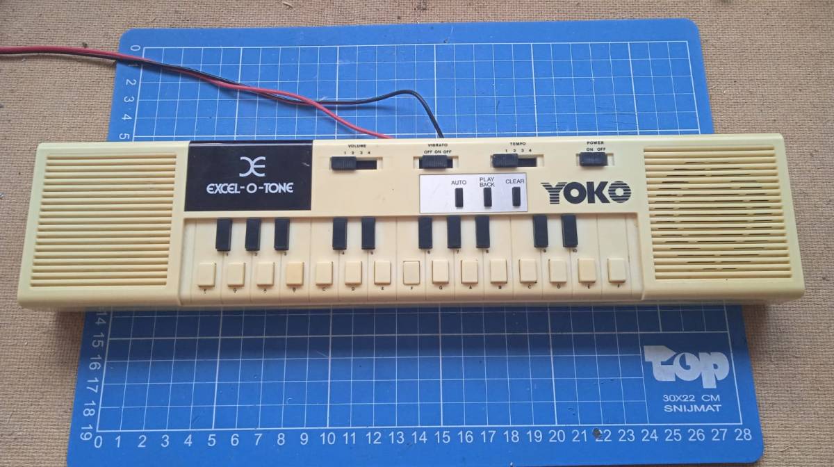
2 euros at the thriftstore, don’t mind if I do! The Excel-O-Tone is pretty much a dumbed down Casio VL-1. It makes monophonic bleep bloop noises with a parrot button that repeats your last played x amount of notes. You can add in vibrato on the bleep bloops and that’s about it. Also I haven’t got a clue what a Yoko is besides an exquisite musician and artist from Japan.
Features
Power on/off switch
25 keys
1 oscillator (monophonic)
4 volume levels
4 tempo levels
Off-On-Off vibrato function
Note sequence repeat button
No clue what the “auto” button does, it just stops all keys from making sound
Headphone output (3.5mm)
Battery powered (4x AA @ 1.5V)
2 extra spots to store batteries for your calculator or something?
DC IN (probably 6v)
Yellowed
Why it sucks
Wonky key response. Keys don’t register when playing too fast, sometimes stutter, sometimes plays an x amount of time even after letting go. Not very musician friendly so to speak.
Vibrato not very convincing, also why is that switch off-on-off?
The sequence repeat function doesn’t take rhythm in account, every note plays for the same duration.
Teardown
First thing we see are two speakers (such a luxury!) a small PCB on the bottom for the DC IN and headphones out and a big PCB on the top which has all the rest.
Zooming in on the interesting part shows us what they use for clock, microcontroller and audio output amp.
My guess is the CD4069 (Hex inverter) has some function as clock for the COP420 (datecode week 8, 1985) that happens to be a 4 bit microcontroller which also handles all the other functionality like the “keyboard” and other switches and buttons.
They chose to use an LM386 (type 1) as driver for the two speakers. Why they use two speakers is a cost-cutting mystery to me as the “synth” is mono. To make matters worse, it seemed like the speakers were connected out of phase which initially gave me acoustic headaches while playing the bleeps and bloops. I decided to swap the wires of one of the speakers to fix that.
Always interesting to see the manually routed single sided boards. If you didn’t know yet, the PCB designs were laid out with tape! This is why the tracks look so wobbly. The keys just use a membrane type-o technology. Nice and cheap. The switches are stuck on the PCB by those black plastic frames. No way to replace them if something were to happen to them!
Note the unused footprint in the top-left corner. Seems like they were also in the process of copying the calculator which could be found on the Casio VL-1.
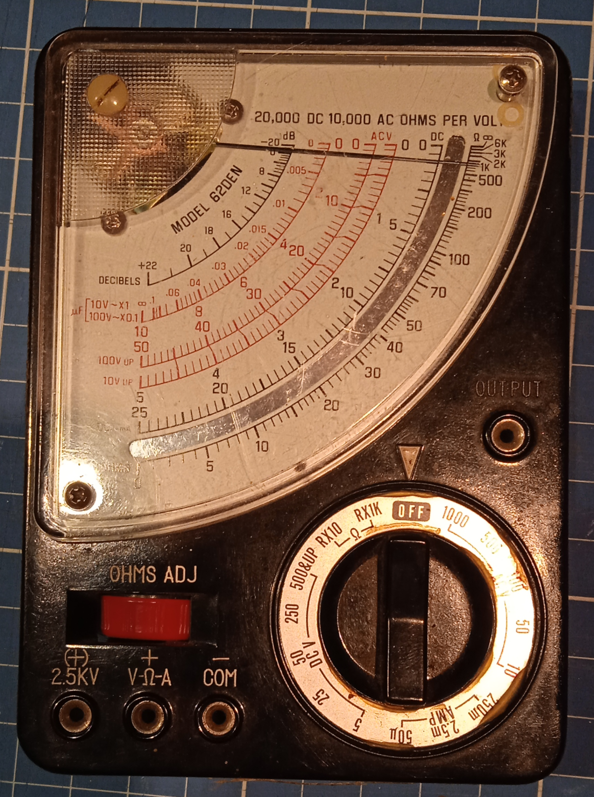
A dumpsterdive from a while back of a heavily beaten vintage multimeter. The enclosure is broken but the electronics still look fine. I can’t get the analog panelmeter to nul to 0 tho with the adjustment on the front of the meter. Maybe there are tricks to get that working and have nice new meter!
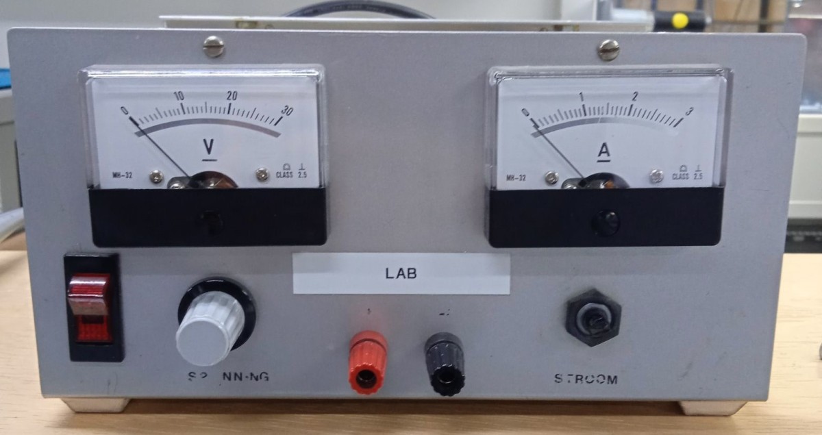
Found this lab bench power supply at work which had a loose current limit pot. So I decided to open it up with the intention to fix this loose pot. But while doing this I might as well document what I could find in there!
Specification
Seems like the PSU is dutch judging by the labels on the front. “Spanning” meaning voltage and “stroom” being current. This also tells us that this is a 30V 3A lab power supply. If anyone knows more about brand, type and year, please contact me 🙂
The outside
Front of the PSU
Two analog panel meters to show voltage and current. I nice chunky power switch with integrated pilot light. Two knobs to set the desired voltage and current limit. And the voltage gets presented at the two banana plug posts that are also screwable to attach wires.
As visible, the knob on the current control pot is removed. I did this so I could reach the nut that makes sure the pot is tight against the chassis and won’t move when the knob is turned or reaches its limits. This nut was loose which led to the knob shifting and rotating around while being operated.
The insides
Top view PSU
In fact not much going on. The panel meters, banana posts and power switch at the top all with nice beefy wires.
Also a nice big transformer with what seems 2 secondary outputs which possibly gets put in series to get a rectified voltage of 33.6V, great for the linear regulators to get the 30v out of.
At the back of the power supply is a connection to mains, a fuse on the primary side and a power transistor (TO-3) which gets mounted on a nice big heatsink out of frame.
Of course the star of the show is the single sided regulator PCB!
Close up of regulator board
There is a big chonky 4700µF smoothing capacitor and a full bridge rectifier in a quite unusual visual arrangement. Probably better for airflow like this.
heatsank socketed DIP IC
I didn’t take the time to remove the heatsink from that DIP IC but it’s most definitely some kind of linear voltage regulator but can also be an opamp. Let’s just admire the view of a heatsank DIP that’s also put on a socket!
One of the transistors, a BD140 accompanying the TO-3 on the back. I’m not sure what TO-3 that is, could be a chonky pass transistor or even a TO-3 LM317.
I will take more pictures and fetch more details whenever I get the chance. If anyone knows more about this PSU, please let me know 🙂
Update!
Here is another batch of pictures, enjoy!
View of the shunt resistor, 0.22 ohms470 and 10k linear pots LM723, up to 40V input, 2 to 37v output linear regulator in DIP (was hidden under the heatsink)External pass transistor, a good ol’ 2N3055 for the needed oomph
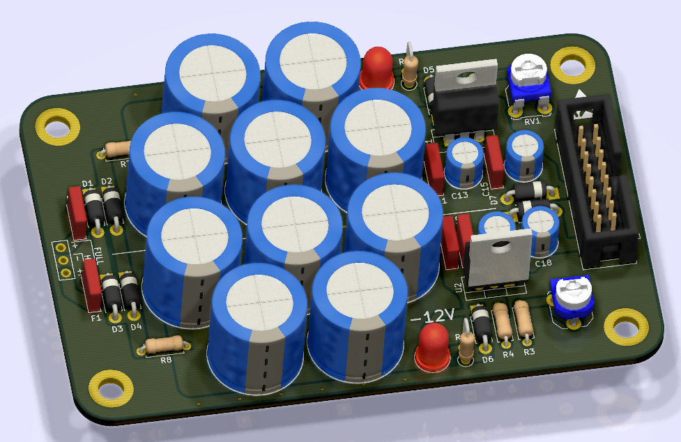
Obviously, without a power supply you get nowhere in synth land. Hence I went out to design a power supply that can deliver positive and negative 12v with decent oomph.
The base design is nothing remarkable but I added some interesting bits to make the supply a bit more versatile or “advanced” so to speak.
The design
It is a bit of a big boy so click on it to see it a bit more up close in a new tab.
The charm is that the design works with both a single 12VAC power supply as a center tapped dual 12VAC power supply. Of course, the latter will have less ripple and other side effects the 12VAC one will have. But 12VAC wall warts can be found at any thrift store or laying around gathering dust on attics. You might be able to source center tapped transformers cheaply from broken audio devices but do this at your own risk.
Higher input AC voltage might work just fine. Just keep an eye on the rectified voltage regarding the capacitors and the added power dissipation by the linear regulators.
Input stage
After we put some AC on the input, we let the current travel through some poly fuses because it’s always a good idea in case of a short circuit event that could happen before the linear regulators, to have some protection.
After this initial protection, we just enter a full bridge rectifier setup that works for both single winding transformers as center tapped ones. After that I placed some resistors marked “Inrush”. They are optional but while we are here, let’s do it the proper way. You can put a low value resistor here if you like wasting energy or an NTC that is high resistance at startup but then slowly goes low resistance as the capacitors are charged.
If you don’t care about this because you keep bulk capacitance low or like to live on the edge, be my guest and put a 0 ohm jumper where the inrush limiting device goes or short the jumper at the back of the board. Placing or doing nothing at all will basically stop the input from reaching the bulk capacitance so make a choice.
Linear regulator
Ah, the fun part! You might be crying at the sight of so many capacitors and so much capacitance. But it’s only a guideline and a way to have freedom to experiment. These rows of capacitors are the bulk capacitance and their main task is to smooth out the dirty full wave or disgusting half wave rectified AC.
I’d say, keep c11 and c12 as they are but add or remove those fat electrolytics to taste. It really depends on your load too and how much ripple you allow at the very output. And please check rated voltage and polarity before you reenact the big bang.
Now the linear regulator is being a bit “abused”. It is pretty much hooked up like a LM317 which means we can alter the output voltage. They are 5V regulators so you expect 5V at the output, but when changing the voltage at what usually is the ground terminal, you can suddenly program the output voltage from 5V to the input voltage.
I use the LM7805 and LM7905 pair because those are in my regulator stash. I just do not own the negative version of the LM317, the LM337. If the tuning of the output voltage is not desired and you are okay with the tolerance on linear regulator output voltages, feel free to replace them with 7812 and 7912 regulators and call it a day. Make sure to follow the directions as shown in the schematic cause it requires some minor mods.
D5, D6, D7 and D8 are the basic reverse voltage event protection diodes which are recommended in every linear regulator datasheet.
Also make sure to put a to-220 compatible heatsink on the regulators cause they might get hot at heavier loads.
Output stage
There is not much to see here. Two LEDs to indicate there is voltage present and optional clamping diodes (well chosen zeners or varistors will do) to limit the output voltage.
Then the power rails are presented to an IDC compatible 16 pin connector of which 6 pins do nothing. So it’s also possible to put a 10 pin IDC connector there.
PCB Design
The PCB design is mostly polygon based to make sure the ampacity of the tracks is alright. Sadly the Kicad is a nightmare with polygon editing as non 45 degree angles are easy to make leading to all kinds of ugly Picassos.
Front view PCBBack view PCB3D view
These PCBs are ordered at JLCPCB October 17th 2021, and once they are here I will update this article.
Update November 7th, PCBs!
It took about 16 days for the PCBs to arrive. They look very good!
Assembled PCBs
Ofcourse, the next thing to do is to solder all the parts to the board and short the solder jumpers.
Assembled PSU
Tests
When I got my lab setup, I will start testing the boards.
I will test the relationship between the load (up to 1A per rail), ripple and output voltage on a half wave rectified input. This is important to get an idea of what capacity is enough and what is too much. This could cut cost drastically.
Once the tests are completed, this article will be updated!
Update January 15 2022
I’ve got the PSU already in use for weeks during prototyping and it works very well. I also did a series of tests to check the ripple and voltage drop under load. With only 4700uF decoupling capacity per rail, I couldn’t manage to get the voltage rails to do anything nasty before the regulator current limiter or the polyfuses kick in.
I found one flaw in the design which I did not see coming. De positive rail can be perfectly trimmed to 12v, also under load. But the -12v rail under the same load can not be fully trimmed back down to -12v. But this can easily be fixed with changing R3 to a higher value. In my case I went to 560 ohm.
While trying to get a versatile LFO going and failing at it… I decided to already go a step further and take a look at attenuverters.
Attenuverters
The concept is easy. With the potentiometer set at 12 o’clock, we get no signal from the input at the output. When rotating the potentiometer to the right, we slowly get our input signal back. Once we reached the limit of the potentiometer, the full input signal is at the output. Important: between 12 o’clock and the mostright limit is an attenuated version of the input signal!
Now if we rotate from 12 o’clock to the left, the same effect happens BUT the signal is inverted! So a sawtooth can be shaped into a ramp and an ADSR can be shaped from a pluck to a sidechain compression effect!
The effect of attenuverting at different potentiometer positions. The rightmost signal was originally at the input.
Offset
Offsetting a signal is the act of adding or subtracting the DC level. This basically just means shifting the whole signal up or down.
This can be very useful to for example set a base control voltage where let’s say, a LFO will swing around. An simple practical patch is to route a 5Hz sinewave (or triangle…) to the input of the attenuverter, then routing the output to a VCO. Now dial in the desired frequency / tone with the offset knob and use the attenuverter control to dial in a slight vibrato!
The effect of offsetting at different potentiometer positions. The middle position is equal to no added offset.
Gain
Now you might think, where do you need gain for? Many attenuverter modules only offer an attenuvert and offset control. Well imagine that your ADSR or LFO has a poor output swing or just doesn’t have the voltage range it needs to? This can be easily solved with a bit of gain!
In my design I don’t have variable or user accessible gain control. I did this on purpose because the attenuvert control will practically control the overal gain. So having the attenuvert potentiometer all the way to the right, won’t give the original input signal, but an amplified version!
This extra gain does make the attenuvert control more sensitive. Tuning in for example a subtle vibrato will not need a lot of travel on the potentiometer, but it surely isn’t impossible to tune in.
The design
Having attenuverting, offsetting and a higher than unity gain makes this design an extremely versatile tool in any synth setup.
Attenuvert and offset and gain schematic
Opamp U1A is the basic attenuverter design. Really nothing special to see here. The big idea is that RV1, depending on potentiometer position, can change the configuration of the opamp from non-inverting to inverting. Hence it does attenuverting. R1 and R2 are optional resistors you can place to make the attenuvert control less finicky around 12 o’clock. I had good results with anything between 10k and 47k but just see for yourself what feels good.
The practice of putting resistors around a potentiometer is called tapering: changing the response of a potentiometer. If you need a bit more precision in the first 40% of a potentiometer or if you need to limit the range of your potentiometer, tapering will often get you very far. And it's cheaper than buying a dedicated potentiometer for it! The internet has enough guides on how to taper a potentiometer to your needs, so try that first before investing in that weird expensive pot!
After attenuvertion the signal is passed on to an inverting amplifier with a gain of x10 due to R7 and R5. A DC offset is injected onto the opamp summing point thanks to R11 and potentiometer RV3. C3 is an optional capacitor to bandwidth limit the opamp to about 20kHz if you so desire. R15 is an optional resistor that limits the drive current of U1B in an output short circuit event.
Scope captures
To show that the schematic actually also works in the real world, I built it up on breadboard and took some scope captures showing the basic functionalities.
The output waveform of a sawtooth generated by a phone cause I lack a proper sawtooth LFO. It is kinda hard to show inversion on a sinewave, squarewave or triangle because of their symmetry, hence I went with the janky sawtooth at a frequency quite higher than the LFO domain. It doesn’t matter as it will still show just fine how the attenuverter works.
In this one the attenuverter potentiometer is rotated the other way around, resulting in an inverted sawtooth -> a ramp.
Here I added some DC offset action which shifts the whole waveform above 0v for VCO or other CV input modules that can’t cope with negative voltages.
Oh no… The LM358! An opamp loved by some, hated by many.
What’s with it?
The LM358 is a dual opamp that isn’t like the other girls. For example, it has the ability to drive its output voltage very close to the negative supply rail. Something we only see in rail-to-rail opamps, but certainly not in other popular dual opamps like the TL072, NE5532, RC4558 and the list goes on and on.
This superpower has its pros: more headroom and range. But the LM358 is also flawed. Besides only being two times noisier than the TL072, it is advertised to be low power and they starved its output stage to achieve this. This means that while other opamps have a clean output stage, the LM358 introduces so called crossover distortion to your beautiful signals.
One half of an LM358, can be divided in 3 stages: Input stage consisting of a differential amplifier, voltage amplification stage (VAS) and the output stage.
This is where some people stop caring for the poor opamp. We do not want distortion in our signals, they shout!
I ran into this problem when I began scoping my first audio circuits, and the internet is saturated with forum threads addressing the issue. The answers are almost always the same too. They say, its crossover distortion, can be apparantly fixed with a resistor to ground (hm… interesting), but the best cure is to bring the opamp back to the museum and let it rest in peace with the non-CMOS 555 timers and vacuüm tubes.
Chineseum
Ofcourse the LM358 wasn’t designed with audio or hifi in mind, but it is such a cheap opamp. This becomes apparent when one gets the urge to order opamps from China. 10 TL072s for less than a dollar!? What a bargain!
Almost 1000 people scammed in the first 3 listings of TL072s on Aliexpress
I hope these people find out that their cheap low noise JFET input opamps are actually LM358s in disguise, ready to scam every naive electronics hobbyist. I can only shiver at the thought of the amount of guitar pedals, amplifiers, synthesizers and other audio devices that are littered with LM358s where the “designer” expected them to be TL072 or equivalent. Oh? what about the quad opamps like the TL074 you got so cheap too? Sorry, they’re probably LM324s: nothing more than a double LM358 in a nice convenient package.
Alright, alright! Yes, also I once naively bought these opamps thinking they were possibly legit. It never occurred to me back then that the TL072 is supposed to be anything special, so the price seemed okay. How could I have known they’re almost the goto opamp for DIY audio projects? I found out they were fake when my waveforms got crossover and the output voltage magically swung near 0V, both these things don’t happen to legit TL072s.
Video I made on verifying if your Chinamps are also fake
Alright cool, but now what?
For its price and availability I want to give the “358” many benefits of the doubt. I was notified of an article by Jack Orman who fails to specify if the scope of his experiment is for guitar pedal usage or actual hifi.
For the record, guitar pedals aren't hifi and stop trying to make them appear hifi. There are so many factors that decide how your tone will sound, that chasing low distortion or whatever is really not worth it. Your amplifier most probably doesn't even have the full bandwidth of audio and better yet, it really doesn't need it either. We thank our guitar tones to imperfections and overall jank. So embrace it, but please put more time in practicing your guitar playing than chasing tone. After all, what's the use of having a 2000 dollar rig when you have 5 dollar skills?
He did some distortion tests with various opamps only to show that the LM358 has crossover. Well, woohoo what a revelation! What’s next? Proving that a battery doesn’t have ripple?
It got me thinking about that resistor to ground again that apparantly can fix crossover. Nowhere on the internet I could find tests or measurements of this. Only this well known video I watched years ago when I stumbled upon these weird bites that were taken out of my waveforms. It proved that the loading of the output indeed does remove the crossover to an extend. But how much loading is too much, what are other caveats? What THD% (total harmonic distortion) are we talking about? I decided to find out myself.
Crossover distortion on a sinewave
The test procedure
The big idea is to run a low distortion 1kHz sinewave from my phone (Yes, your phone is possibly a very good source for low distortion sinewaves when using the right app!) through the LM358, and feed the output to my audio interface (Focusrite 2i2 2nd generation). ARTA will then analyze the incoming signal with a spectrum analysis.
The LM358 will get a bit of gain to make sure the lousy phone signal is a bit oomphier while at the same time making sure that the output signal is more sinewave than crossover distortion. I ended up using a gain of 11 which was equal to an output signal of about 4.5Vpp.
ARTA will be set up with:
Fs (samplerate): 48kHz (more than enough for 1kHz and the audio band)
FFT size: 32768 (about 1 measurement/second, I don’t have all day)
Window: Kaiser 7 (recommended for 24 bit harmonic distortion measurements)
Averaging: 50x linear (but feel free to do more averages if you so desire)
I also use a capture of the spectrum with no signal which can be later used to cancel any parasitic mains hum and other nastiness from the measurements.
You can make one yourself by starting a measurement without the 1kHz test signal, then exporting it as file -> export -> ASCII file. Then go to setup -> FR compensation and load this .TXT file back up. Tick the “use for spectrum” box and you’re good to go. Note that the measurements from here onwards will be around 0dB and higher due to the compensation!
I will first also test some other opamps that don’t have silly output stages as comparison.
Test setup
The opamp circuitry is as follows:
As visible a simple non inverting amplifier with a gain of 11. I’m working with a single 9V supply so the input has to be biased to half the supply voltage (otherwise you clip the negative half of the incoming AC). This is done with voltage divider R1 and R2 where R3 injects this DC voltage onto the AC. C1 decouples this reference voltage to keep it nice and quiet.
To make sure the amplifier doesn’t amplify the DC offset with the AC, capacitor C3 is added to add some high pass action to the amplifier. This way DC is ignored and you get the amplified AC (still with a nice 4.5V DC offset) at the output. C4 and R6 make sure the DC offset is removed so an AC signal centered around 0V gets send to the audio interface.
To make sure the 2nd opamp in the package doesn’t ruin our day, it gets terminated. This is properly done by configuring it as voltage follower/buffer where the to be buffered voltage is a voltage anywhere between 9V and ground. Luckily we have exactly such a thing thanks to the voltage divider!
R7 will be replaced by various values to experiment with the loading of the opamp. The big idea here is that pulling current out of the opamp forces a class A operation from the output stage. And you know what that means, crossover begone!
Measurements!
Hold your horses. First we need to find out how shitty our test setup is. I do this by first checking how good my sinewave generator is by hooking it up straight to the audio interface without any type of compensation:
THIS IMAGE GOT LOST AND CORRUPTED SO I REPURPOSED THE JRC4558
Oh my lordy lord. What a beauty!
Next up, testing some non “358 core” opamps. I got quite a stash, some legit, some from China. I will tell which ones are which…
JRC4558 measurement
Here we have a China JRC4558 which means that it’s probably something else. As you can see it is quite clean tho, which is a good sign. The fuzz at around the noisefloor is I don’t know what, maybe artifacts from the compensation but it is not important.
Just notice how theres a nice peak at 1kHz, and then a 2nd harmonic at double the frequency. Later on in the spectrum at 15k and 17k are some peaks too. They’re related to the input sinewave yet don’t make much sense there. Maybe aliasing?
LF353 measurement
Here I replaced the 4558 with a legit LF353. A little bit less fuzzy with quite a similar pattern in harmonics. Again very low distortion.
NE5532 measurement
A China NE5532 aka no clue if it is legit. Similar spectrum to the other opamps with a low distortion and noisefloor.
LM358 with no load resistor
Oh boy! Is this a squarewave? No, don’t worry its not that bad. Just an LM358 doing its thing. As you can clearly see the crossover adds a good amount of harmonics compared to the others.
Now let’s see how it cleans up when we add the load resistor with less and less resistance!
LM358 with 100k load
In this one a 100k resistor is placed straight from the output to ground. Seems like it’s just too big to matter. The current drawn by the whole circuit is 1.12mA. Let’s reduce that resistor!
LM358 with 10k load
10 times heavier load. Still not that much reduction. The fourth harmonic seems to be a bit quieter tho. For the total THD it really doesn’t matter and believe me, you won’t hear the difference. The total current draw is 1.35mA so there’s at least something happening. Next!
LM358 with 1k load
Pardon me? Distortion, where did you go? Now isn’t this juicy! 10x heavier load and a performance like any other opamp! The total current draw went towards 5.03mA though, yikes!
Going too far with the loading will just result in the output getting shorted to ground and having no signal whatsoever with a good amount of current draw. Useless.
Maybe we can sort of finetune the load anywhere between 10k and 1k and at least see where the higher harmonics start to die out? I put in a 10k linear potentiometer and slowly increased the load until the harmonics started to go away. This was roughly around 4.8k ohm.
The process of turning this pot from 10k to 0 ohms is visible in the animation below:
The measurements for THD are off with the ones on the previous measurements because this GIF is recorded with ARTA sampling at a lower FFT resolution. Notice how we start off with the original harmonics, they start to dance a little but then slowly die out to neglectible levels. After that the whole noisefloor jumps because we shorted the whole thing to ground which scares ARTA.
For my next trick I tried to tune the THD towards a respectable 0.1% but this can be quite hard with 50 averages happening. So I decided to tune it until the total current draw of the circuit was 2mA.
LM358 with 3.8k ohm load
It looks bad but the measurements don’t lie (or do they?).
In conclusion
TLDR; The LM358 is a tradeoff between THD and power consumption.
Do with the information what you want. All I care for is that I tried to show the internet some stuff they might’ve not seen before, or do not have the gear (or motivation, time, lack of pretentiousness) for to check.
To me it seems like the LM358 is a worthy candidate now for many projects even in audio. But then again, one could also just easily invest in opamps that are only a tiny bit more expensive, but improve by miles in performance.
But what else will you do with all your fake opamps?
During the synthesizer building journey, I was looking for a VCO with a V/OCT control voltage input. Quite quickly I stumble upon the designs by René Schmitz. My eye fell on a VCO that utilizes a 4069 hex interver IC. I have quite some of those laying around, and as the design doesn’t use any other exotic components, I decided to give it a go.
The design
I drew the schematic in Kicad so I could later on turn it easily into a perfboard layout.
I changed a few things but not much:
The pots were 22k which to me just sounds odd. I lowered them to a more commonly available 20k.
Output caps for the waveforms are way higher. Not for a particular reason. I just own a lot of 10µF capacitors.
The design also shows the usage of 10k thermistors (NTC). I sourced mine from China as I wasn’t in the mood to pay good bucks for “special synthesizer approved” thermistors. I’ve yet to find out if they really play that much of a role in this design or could’ve easily been omitted.
Perfboard layout
After laying out the schematic, I translate all the components to footprints that all obey a 0.1″ or 2.54mm pinspacing. Depending on the space and efficiency, I have resistors and diodes that “stand upright” so they only cover 2 pads, instead of 4.
The base layout is copied from Schmitz, with some alterations here and there. Green connections pretty much mean a jumper wire.
As you can see, in the upper left corner of the board is the exponential converter. Because I used a 2N3904 and 2N3906, they aren’t facing eachother. This might have an impact on the temperature stability. My guess is that I can easily replace them with transistor types with mirrored pinouts, so I can just have them face to face and glue them down.
Those with a keen eye will see that the potentiometers are missing. That’s right. I usually treat them as an afterthought to be solved by jumperwires.
Perfboard / protoboard
With the layout done, it was time to transfer it to protoboard. I’ve yet to find out if I love or hate protoboard. I find it often to be a miserably tiresome way to get your electronics projects going. Sadly PCBs will cost more money (not a lot, but still more money) and vero or stripboard just makes me puke.
Tuning
Yes this design isn’t very temperature stable, and I also didn’t try my best to make it better. During the tuning process I did tie the two transistors together so their enclosures touch. But even thinking about a holiday is Spain makes them drift a few cents.
Anyway, this was the first time I tried tuning a VCO and had no clue what the procedure was. So I just did what seemed logical. I set the 1k trimmer pot about halfway, the external CV source on 1VDC and tuned the output with the CV pot to be about 200Hz. I was quite sceptical of my approach so I didn’t bother going for precision or a logical starting frequency. I just wanted to confirm my approach.
With 1V being about 200Hz, I started setting the CV to 2V, then 3V, … 5V. 5 octaves should be quite enough, right? Every time the frequency was off, I adjusted it with the trimpot. Then went down again, and up, until I was quite satisfied with the tuning. One value I missed was 0V, so I slammed down the CV and saw the frequency going beautifully to somewhere quite close to 100Hz.
I noted the sweep in a graph, voltage on the X axis and frequency on the Y:
I guess for a more musical approach, one should take a bit more time and care in the tuning process and get it close to bang on. But this graph already tells me that there is a lot of potential in this VCO.
Waveforms
Here are some quick and dirty images of the waveforms:
Squarewave / pulse @ 50% PW, 400Hz (Clipping the audio interface input, oops!)Squarewave / pulse @ not 50% PW, 400Hz (Also clipping the audio interface…)Sawtooth @ 400Hz
When you get into synthesizers (or any other analog audio related topic), you quite quickly come across designs like VCAs with long tailed pair (LTP) input stages or the famous ladder filters that require you to have so called “matched” transistors. Transistors are usually quite variable (just measure some Hfe (beta) of some to find out), but less variable than lets say, JFETS. Still for these applications you need to find pairs that will somewhat behave the same.
So I looked in my BJT drawer and found a nice bag of 2N3904 NPN bipolar transistors I bought years ago from good ol’ China. The bad thing is that these might not even be 2N3904 transistors, the good thing is that they behave like general purpose transistors for the past few years.
So I randomly took 20 of them out the bag and decided to see how the matching procedure is like. The first test setup I found was “apparantly” used by Moog to find matches. Well, that gotto go right, right?
Ofcourse I used the one for the NPN transistor. I didn’t really care much for the precision of the used resistors and tried to get the power supply as close as possible to +-10v. I ended up with a stable current of 106µA, guess that is close enough!
Ofcourse don’t handle the transistors with your fingers and give them some time to get to ambient temperature. Transistor parameters are heavily temperature dependent (also one of the reason we try to match them).
Moving the test leads from one transistor to the other is safer than moving the transistors to the test leads. All just to make sure they stay at ambient temperature.
So I measured the Vbe of the 20 transistors and wrote the voltage down in millivolts (mV):
Alright, they’re all already fairly close it seems. Maybe a bit too close…
I got sceptical so wanted to retry the test with another multimeter (the one I used first is a no brand China one that usually doesn’t betray me…). So I grouped the 20 transistors per value as in the picture above.
Then did the measurement again, but with the other multimeter. Suddenly all values were a steady 30mV higher. Now that is nightmare fuel!
The “big” number is the millivolts the transistors gave me with the cheapo meter. Now it seems like each transistor gave another spread for every group. Seems more realistic, so I got hope again. But this is not where I wanted to stop.
I decided to group the ones that match again, and let them fight in a transistor battle to death.
Basically I used another test setup that lets you test and compare two transistors at once…
Nothing much to see here, it’s just important to get stable power supply rails and match the 100k resistors to be decently matched. This should be rather easy in 2021. D1 was in my case just a general purpose 1N4148.
If the transistors are perfectly matched, the voltage from emitter to emitter should be 0V. If the transistors are unmatched, a voltage difference will build up and be visible on the multimeter.
Visible is what the difference in voltage was that showed up on the multimeter. Must say it is quite impressive and immediatly turned on my scepticism again.
Ofcourse it might’ve been better to get a multimeter that could measure smaller than 1mV steps (with an unknown precision, didn’t bother to check it), but if the results are already this small (the Moog test setup has matches pass at +-2mV differences!) I am not sure how a more precise multimeter will even matter.
Is matching of transistors something we should care about in 2021? Do Chinese mystery transistors come matched off of the boat? Am I happy with the results?
All questions I don’t quite have an answer on. But for now, bag it and tag it!
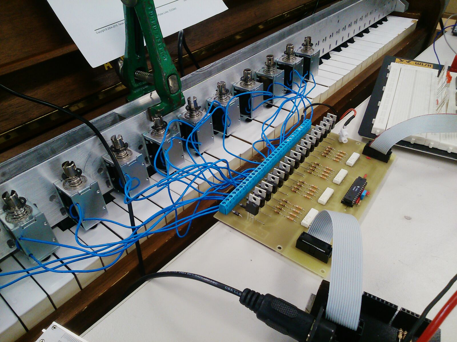
Context For one of the last big projects at my university, me and some colleagues took on the challenge to create a self playing piano also called the PianoPlayer. The PianoPlayer is a stand-alone module that can be placed on any acoustic piano and uses MIDI to play the 88 keys and controls the sustain pedal with a seperate pedal motor module.
MIDI to solenoid Pressing the keys on the piano is done with 88 solenoids. Each solenoid is responsible for one key of the piano. With the use of PWM it’s also possible to introduce velocity which gives the PianoPlayer a human feel. The timing of the keys and the velocity is determined via the MIDI protocol. The MIDI data is processed with the Arduino development environment. The goal is that any device that can output MIDI data to the PianoPlayer (like a keyboard or a computer with a MIDI interface), can play the piano it is placed on.
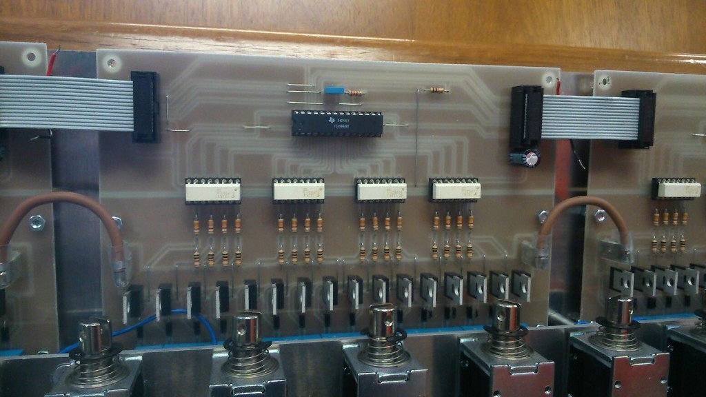
To control all solenoids from one tiny microcontroller, six PCBs (Printed Circuit Board) will be made which contains the analog circuitry to power each solenoid with 48 volts. On each of the six PCBs is also an isolated digital segment which consists of secret switching logic.
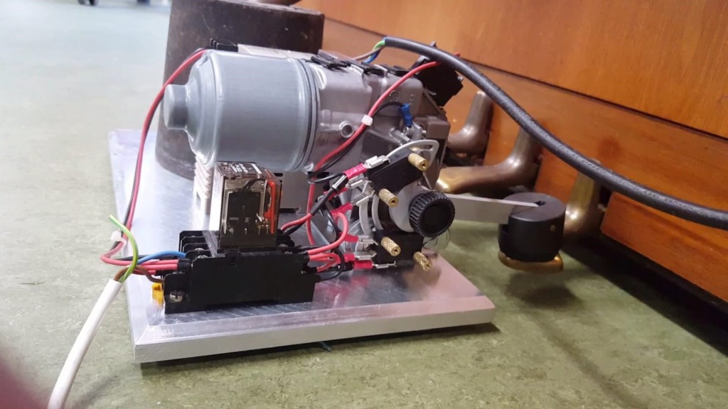
Adding sustain Pianos have a pedal which is called the sustain pedal. This pedal makes sure that any pressed key will ring until the pedal is lifted. To automatically control this pedal, a windscreen wiper motor is customized both electrically and mechanically.
Final result The PianoPlayer is still in development and is planned to be finished in June 2018. The PianoPlayer is already able to:
– Play 10 keys through MIDI
– Control the sustain pedal through MIDI
BUT WAIT! THERE’S AN UPDATE!
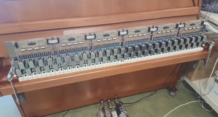
At this moment the PianoPlayer is already finished for months but I never bothered to update this page. The project is a great succes and works like a charm. The pictures below shows the complete setup of the PianoPlayer:
Complete setup of the PianoPlayer. 88 solenoids divided over 6 PCBs.
A close-up of one of the solenoid driver PCBs
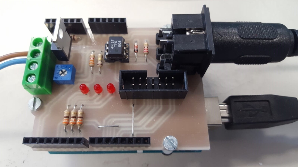
A custom Arduino Uno shield for MIDI input and solenoid and sustain pedal control
The automated sustain pedal. A windscreen wiper motor is reused for this purpose!
DEMO – Flight Of The Bumblebee
The REAL final result The last time I talked about this project the requirements for the Pianoplayer were:
– Play 10 keys through MIDI
– Control the sustain pedal through MIDI
Now we’ve improved this to:
– Play 88 keys through MIDI
– Control the sustain pedal through MIDI